- 您现在的位置:买卖IC网 > Sheet目录1998 > ICS874001AGI-02LF (IDT, Integrated Device Technology Inc)IC PCI EXPRSS/JITT ATTEN 20TSSOP
DATA SHEET
ICS874001AGI-02 REVISION A AUGUST 30, 2010
1
2010 Integrated Device Technology, Inc.
PCI Express Jitter Attenuator
ICS874001I-02
General Description
The ICS874001I-02 is a high performance Jitter Attenuator designed
for use in PCI Express systems. In some PCI Express systems,
such as those found in desktop PCs, the PCI Express clocks are
generated from a low bandwidth, high phase noise PLL frequency
synthesizer. In these systems, a jitter attenuator may be required to
attenuate high frequency random and deterministic jitter
components from the PLL synthesizer and from the system board.
The ICS874001I-02 has two different PLL bandwidth modes: 2MHz
and 3MHz. The 2MHz mode will provide maximum jitter attenuation,
but with higher PLL tracking skew and spread spectrum modulation
from the motherboard synthesizer may be attenuated. The 3MHz
bandwidth provides the best tracking skew and will pass most
spread profiles, but the jitter attenuation will not be as good as the
lower bandwidth mode. The 874001I-02 can be set for different
modes using the F_SELx pins, as shown in Table 3C.
The ICS874001I-02 uses IDT’s 3RD Generation FemtoClock
PLL technology to achieve the lowest possible phase noise. The
device is packaged in a small 20-pin TSSOP package, making it
ideal for use in space constrained applications such as PCI Express
add-in cards.
Features
One differential LVDS output pair
One differential clock input
CLK, nCLK can accept the following differential input levels:
LVPECL, LVDS, LVHSTL, HCSL, SSTL
Input frequency range: 98MHz to 128MHz
Output frequency range: 98MHz to 640MHz
VCO range: 490MHz - 640MHz
Cycle-to-cycle jitter: 15ps (maximum), 3.3V
RMS period jitter: 3ps (maximum), 3.3V
Two bandwidth modes allow the system designer to make jitter
attenuation/tracking skew design trade-offs
Full 3.3V or 2.5V operating supply
-40°C to 85°C ambient operating temperature
Available in lead-free (RoHS 6) package
PLL Bandwidth Control Table
PLL_SEL Control Table
BW_SEL
0 = PLL Bandwidth: 2MHz (default)
1 = PLL Bandwidth: 3MHz
PLL_SEL
0 = Bypass
1 = VCO (default)
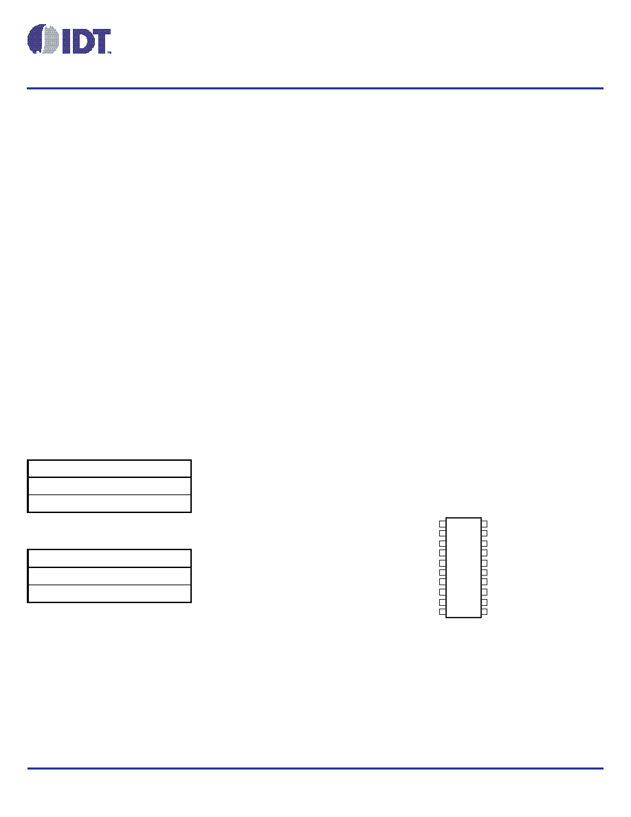
1
2
3
4
5
6
7
8
9
10
20
19
18
17
16
15
14
13
12
11
F_SEL0
VDDA
F_SEL1
BW_SEL
MR
nc
PLL_SEL
VDD
nc
VDDO
Q
nQ
nc
GND
nCLK
CLK
OE
Pin Assignment
ICS874001I-02
20-Lead TSSOP
6.5mm x 4.4mm x 0.925mm package body
G Package
Top View
发布紧急采购,3分钟左右您将得到回复。
相关PDF资料
ICS874001AGI-05LFT
IC PCI EXPRSS/JITT ATTEN 20TSSOP
ICS874002AGLFT
IC PCI EXPRSS/JITT ATTEN 20TSSOP
ICS874005AG-04LFT
IC PCI EXPRSS/JITT ATTEN 24TSSOP
ICS874005AGLFT
IC PCI EXPRSS/JITT ATTEN 24TSSOP
ICS8741004AGLFT
IC PCI EXPRSS/JITT ATTEN 24TSSOP
ICS87604AGILF
IC CLK MULT/ZD BUFFER 28-TSSOP
ICS8761CYLFT
IC CLK GEN PCI/PCI-X 64-LQFP
ICS87946AYILFT
IC CLOCK GENERATOR 32-LQFP
相关代理商/技术参数
ICS874001AGI-02LFT
功能描述:IC PCI EXPRSS/JITT ATTEN 20TSSOP RoHS:是 类别:集成电路 (IC) >> 时钟/计时 - 专用 系列:FemtoClock™, PCI Express™ (PCIe) 标准包装:1,500 系列:- 类型:时钟缓冲器/驱动器 PLL:是 主要目的:- 输入:- 输出:- 电路数:- 比率 - 输入:输出:- 差分 - 输入:输出:- 频率 - 最大:- 电源电压:3.3V 工作温度:0°C ~ 70°C 安装类型:表面贴装 封装/外壳:28-SSOP(0.209",5.30mm 宽) 供应商设备封装:28-SSOP 包装:带卷 (TR) 其它名称:93786AFT
ICS874001AGI-05LF
功能描述:IC PCI EXPRSS/JITT ATTEN 20TSSOP RoHS:是 类别:集成电路 (IC) >> 时钟/计时 - 专用 系列:FemtoClock™, PCI Express™ (PCIe) 标准包装:1 系列:- 类型:时钟/频率发生器,多路复用器 PLL:是 主要目的:存储器,RDRAM 输入:晶体 输出:LVCMOS 电路数:1 比率 - 输入:输出:1:2 差分 - 输入:输出:无/是 频率 - 最大:400MHz 电源电压:3 V ~ 3.6 V 工作温度:0°C ~ 85°C 安装类型:表面贴装 封装/外壳:16-TSSOP(0.173",4.40mm 宽) 供应商设备封装:16-TSSOP 包装:Digi-Reel® 其它名称:296-6719-6
ICS874001AGI-05LFT
功能描述:IC PCI EXPRSS/JITT ATTEN 20TSSOP RoHS:是 类别:集成电路 (IC) >> 时钟/计时 - 专用 系列:FemtoClock™, PCI Express™ (PCIe) 标准包装:1,500 系列:- 类型:时钟缓冲器/驱动器 PLL:是 主要目的:- 输入:- 输出:- 电路数:- 比率 - 输入:输出:- 差分 - 输入:输出:- 频率 - 最大:- 电源电压:3.3V 工作温度:0°C ~ 70°C 安装类型:表面贴装 封装/外壳:28-SSOP(0.209",5.30mm 宽) 供应商设备封装:28-SSOP 包装:带卷 (TR) 其它名称:93786AFT
ICS874002AGLF
功能描述:IC JITTER ATTENUATOR 20-TSSOP RoHS:是 类别:集成电路 (IC) >> 时钟/计时 - 专用 系列:HiPerClockS™, PCI Express® (PCIe) 标准包装:1 系列:- 类型:时钟/频率发生器,多路复用器 PLL:是 主要目的:存储器,RDRAM 输入:晶体 输出:LVCMOS 电路数:1 比率 - 输入:输出:1:2 差分 - 输入:输出:无/是 频率 - 最大:400MHz 电源电压:3 V ~ 3.6 V 工作温度:0°C ~ 85°C 安装类型:表面贴装 封装/外壳:16-TSSOP(0.173",4.40mm 宽) 供应商设备封装:16-TSSOP 包装:Digi-Reel® 其它名称:296-6719-6
ICS874002AGLFT
功能描述:IC PCI EXPRSS/JITT ATTEN 20TSSOP RoHS:是 类别:集成电路 (IC) >> 时钟/计时 - 专用 系列:HiPerClockS™, PCI Express® (PCIe) 标准包装:1,500 系列:- 类型:时钟缓冲器/驱动器 PLL:是 主要目的:- 输入:- 输出:- 电路数:- 比率 - 输入:输出:- 差分 - 输入:输出:- 频率 - 最大:- 电源电压:3.3V 工作温度:0°C ~ 70°C 安装类型:表面贴装 封装/外壳:28-SSOP(0.209",5.30mm 宽) 供应商设备封装:28-SSOP 包装:带卷 (TR) 其它名称:93786AFT
ICS874003AG-02LF
功能描述:IC JITTER ATTENUATOR 20-TSSOP RoHS:是 类别:集成电路 (IC) >> 时钟/计时 - 专用 系列:HiPerClockS™, FemtoClock™, PCI Express® (PCIe) 标准包装:1 系列:- 类型:时钟/频率发生器,多路复用器 PLL:是 主要目的:存储器,RDRAM 输入:晶体 输出:LVCMOS 电路数:1 比率 - 输入:输出:1:2 差分 - 输入:输出:无/是 频率 - 最大:400MHz 电源电压:3 V ~ 3.6 V 工作温度:0°C ~ 85°C 安装类型:表面贴装 封装/外壳:16-TSSOP(0.173",4.40mm 宽) 供应商设备封装:16-TSSOP 包装:Digi-Reel® 其它名称:296-6719-6
ICS874003AG-02LFT
功能描述:IC PCI EXPRSS/JITT ATTEN 20TSSOP RoHS:是 类别:集成电路 (IC) >> 时钟/计时 - 专用 系列:HiPerClockS™, FemtoClock™, PCI Express® (PCIe) 标准包装:1,500 系列:- 类型:时钟缓冲器/驱动器 PLL:是 主要目的:- 输入:- 输出:- 电路数:- 比率 - 输入:输出:- 差分 - 输入:输出:- 频率 - 最大:- 电源电压:3.3V 工作温度:0°C ~ 70°C 安装类型:表面贴装 封装/外壳:28-SSOP(0.209",5.30mm 宽) 供应商设备封装:28-SSOP 包装:带卷 (TR) 其它名称:93786AFT
ICS874003AG-04LF
功能描述:IC PCI EXPRSS/JITT ATTEN 20TSSOP RoHS:是 类别:集成电路 (IC) >> 时钟/计时 - 专用 系列:HiPerClockS™, FemtoClock™, PCI Express® (PCIe) 标准包装:1,500 系列:- 类型:时钟缓冲器/驱动器 PLL:是 主要目的:- 输入:- 输出:- 电路数:- 比率 - 输入:输出:- 差分 - 输入:输出:- 频率 - 最大:- 电源电压:3.3V 工作温度:0°C ~ 70°C 安装类型:表面贴装 封装/外壳:28-SSOP(0.209",5.30mm 宽) 供应商设备封装:28-SSOP 包装:带卷 (TR) 其它名称:93786AFT